- 您现在的位置:买卖IC网 > Sheet目录3876 > PIC18F14K50-I/SS (Microchip Technology)IC PIC MCU FLASH 8KX16 20-SSOP
PIC18F/LF1XK50
DS41350E-page 108
Preliminary
2010 Microchip Technology Inc.
11.3.2
TIMER1 OSCILLATOR LAYOUT
CONSIDERATIONS
The Timer1 oscillator circuit draws very little power
during operation. Due to the low-power nature of the
oscillator, it may also be sensitive to rapidly changing
signals in close proximity.
The oscillator circuit, shown in Figure 11-3, should be
located as close as possible to the microcontroller.
There should be no circuits passing within the oscillator
circuit boundaries other than VSS or VDD.
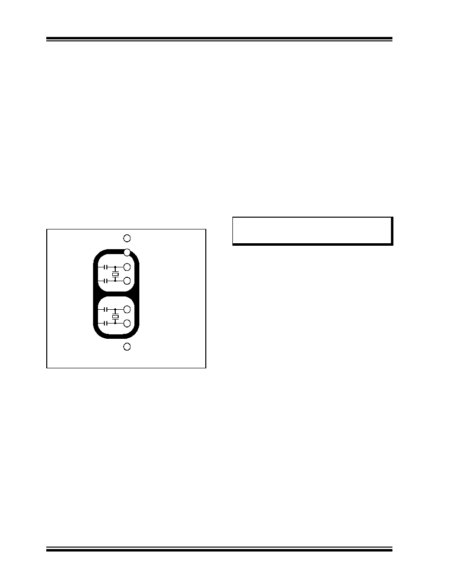
If a high-speed circuit must be located near the oscilla-
tor (such as the CCP1 pin in Output Compare or PWM
mode, or the primary oscillator using the OSC2 pin), a
grounded guard ring around the oscillator circuit, as
shown in Figure 11-4, may be helpful when used on a
single-sided PCB or in addition to a ground plane.
FIGURE 11-4:
OSCILLATOR CIRCUIT
WITH GROUNDED
GUARD RING
11.4
Timer1 Interrupt
The TMR1 register pair (TMR1H:TMR1L) increments
from 0000h to FFFFh and rolls over to 0000h. The
Timer1 interrupt, if enabled, is generated on overflow,
which is latched in the TMR1IF interrupt flag bit of the
PIR1 register. This interrupt can be enabled or disabled
by setting or clearing the TMR1IE Interrupt Enable bit
of the PIE1 register.
11.5
Resetting Timer1 Using the CCP
Special Event Trigger
If either of the CCP modules is configured to use Timer1
and generate a Special Event Trigger in Compare mode
(CCP1M<3:0> or CCP2M<3:0> = 1011), this signal will
reset Timer1. The trigger from CCP2 will also start an
A/D conversion if the A/D module is enabled (see
information).
The module must be configured as either a timer or a
synchronous counter to take advantage of this feature.
When used this way, the CCPRH:CCPRL register pair
effectively becomes a period register for Timer1.
If Timer1 is running in Asynchronous Counter mode,
this Reset operation may not work.
In the event that a write to Timer1 coincides with a
special Event Trigger, the write operation will take
precedence.
VDD
OSC1
VSS
OSC2
RC0
RC1
RC2
Note: Not drawn to scale.
Note:
The Special Event Triggers from the
CCP2 module will not set the TMR1IF
interrupt flag bit of the PIR1 register.
发布紧急采购,3分钟左右您将得到回复。
相关PDF资料
PIC24F08KL302-I/ML
IC MCU 16BIT 8KB FLASH 28-QFN
PIC24F08KL302-I/MQ
IC MCU 16BIT 8KB FLASH 28-QFN
PIC16LF627A-I/P
IC MCU FLASH 1KX14 EEPROM 18DIP
PIC18F25K20-I/SO
IC PIC MCU FLASH 16KX16 28SOIC
PIC24F08KL301-I/SO
IC MCU 16BIT 8KB FLASH 20-SOIC
PIC24F04KL101-I/P
IC MCU 16BIT 4KB FLASH 20-PDIP
PIC16LC56A-04/SO
IC MCU OTP 1KX12 18SOIC
PIC16LF74-I/PTG
IC MCU FLASH 4KX14 44TQFP
相关代理商/技术参数
PIC18F14K50T-I/SO
功能描述:8位微控制器 -MCU 16KB Flash 768 RAM15 I/O 10-B ADC USB 2.0
RoHS:否 制造商:Silicon Labs 核心:8051 处理器系列:C8051F39x 数据总线宽度:8 bit 最大时钟频率:50 MHz 程序存储器大小:16 KB 数据 RAM 大小:1 KB 片上 ADC:Yes 工作电源电压:1.8 V to 3.6 V 工作温度范围:- 40 C to + 105 C 封装 / 箱体:QFN-20 安装风格:SMD/SMT
PIC18F14K50T-I/SS
功能描述:8位微控制器 -MCU 16KB Flash 768 RAM15 I/O 10-B ADC USB 2.0
RoHS:否 制造商:Silicon Labs 核心:8051 处理器系列:C8051F39x 数据总线宽度:8 bit 最大时钟频率:50 MHz 程序存储器大小:16 KB 数据 RAM 大小:1 KB 片上 ADC:Yes 工作电源电压:1.8 V to 3.6 V 工作温度范围:- 40 C to + 105 C 封装 / 箱体:QFN-20 安装风格:SMD/SMT
PIC18F2220-E/SO
功能描述:8位微控制器 -MCU 4KB 512 RAM 25 I/O RoHS:否 制造商:Silicon Labs 核心:8051 处理器系列:C8051F39x 数据总线宽度:8 bit 最大时钟频率:50 MHz 程序存储器大小:16 KB 数据 RAM 大小:1 KB 片上 ADC:Yes 工作电源电压:1.8 V to 3.6 V 工作温度范围:- 40 C to + 105 C 封装 / 箱体:QFN-20 安装风格:SMD/SMT
PIC18F2220-E/SP
功能描述:8位微控制器 -MCU 4KB 512 RAM 25 I/O RoHS:否 制造商:Silicon Labs 核心:8051 处理器系列:C8051F39x 数据总线宽度:8 bit 最大时钟频率:50 MHz 程序存储器大小:16 KB 数据 RAM 大小:1 KB 片上 ADC:Yes 工作电源电压:1.8 V to 3.6 V 工作温度范围:- 40 C to + 105 C 封装 / 箱体:QFN-20 安装风格:SMD/SMT
PIC18F2220-I/SO
功能描述:8位微控制器 -MCU 4KB 512 RAM 25 I/O RoHS:否 制造商:Silicon Labs 核心:8051 处理器系列:C8051F39x 数据总线宽度:8 bit 最大时钟频率:50 MHz 程序存储器大小:16 KB 数据 RAM 大小:1 KB 片上 ADC:Yes 工作电源电压:1.8 V to 3.6 V 工作温度范围:- 40 C to + 105 C 封装 / 箱体:QFN-20 安装风格:SMD/SMT
PIC18F2220-I/SO
制造商:Microchip Technology Inc 功能描述:IC 8BIT FLASH MCU 18F2220 SOIC28
PIC18F2220-I/SOC03
制造商:Microchip Technology Inc 功能描述:
PIC18F2220-I/SP
功能描述:8位微控制器 -MCU 4KB 512 RAM 25 I/O RoHS:否 制造商:Silicon Labs 核心:8051 处理器系列:C8051F39x 数据总线宽度:8 bit 最大时钟频率:50 MHz 程序存储器大小:16 KB 数据 RAM 大小:1 KB 片上 ADC:Yes 工作电源电压:1.8 V to 3.6 V 工作温度范围:- 40 C to + 105 C 封装 / 箱体:QFN-20 安装风格:SMD/SMT